Electron channeling contrast tomography (ECCT): dislocation tomography enabled by ECCI
Scripta Materialia, 2026, 277, 117234 DOIDevelopment and formalization of advanced electron microscopy techniques
I develop and formalize advanced electron microscopy techniques to characterize crystalline defects inside bulk materials — from the theoretical modelling of diffraction contrast to automated dislocation mapping and 3D non-destructive tomography.
My research focuses on linking micro- and nano-structures to the behavior of materials. We use and continuously improve advanced microscopy techniques, with a core expertise in Scanning Electron Microscope (SEM) based methods — particularly Electron Channeling Contrast Imaging (ECCI).
Transmission Electron Microscope (TEM)
TEMTEM allows us to examine extremely small defects inside materials, down to the nanoscale. By studying these tiny flaws in ultra-thin samples, we can better understand how materials behave in real-world applications, such as in engines or structural components.
Scanning Electron Microscope (SEM)
SEMWith SEM, we inspect material surfaces to identify cracks, roughness, or other signs of degradation. It provides a highly detailed view, helping us understand how materials degrade or fail under mechanical stress.
Electron Backscatter Diffraction (EBSD)
SEM techniqueEBSD is an SEM-based method that maps the crystallographic orientation, grain boundaries, and phases within a material. It reveals how crystals orient, shift, or transform when the material is deformed, heated, or subjected to other conditions. This information is crucial for assessing not only strength and flexibility but also phase distribution, texture, and microstructural evolution.
High-Resolution EBSD (HR-EBSD)
SEM techniqueThis advanced SEM technique measures minuscule strains and rotations within crystals, revealing hidden stresses that could lead to failure. HR-EBSD helps us detect weak spots and understand how stress accumulates at a near-atomic level.
Electron Channeling Contrast Imaging (ECCI)
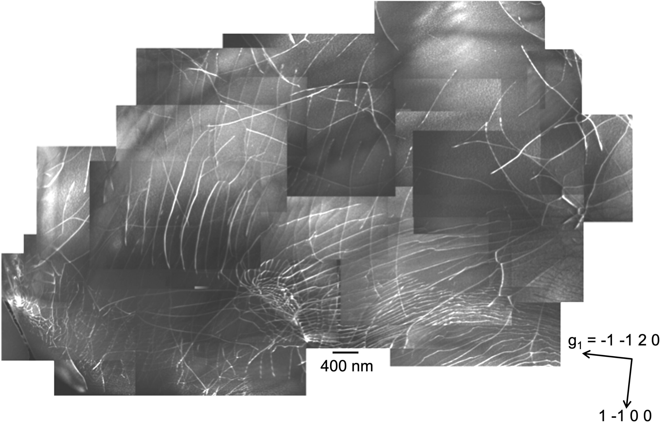
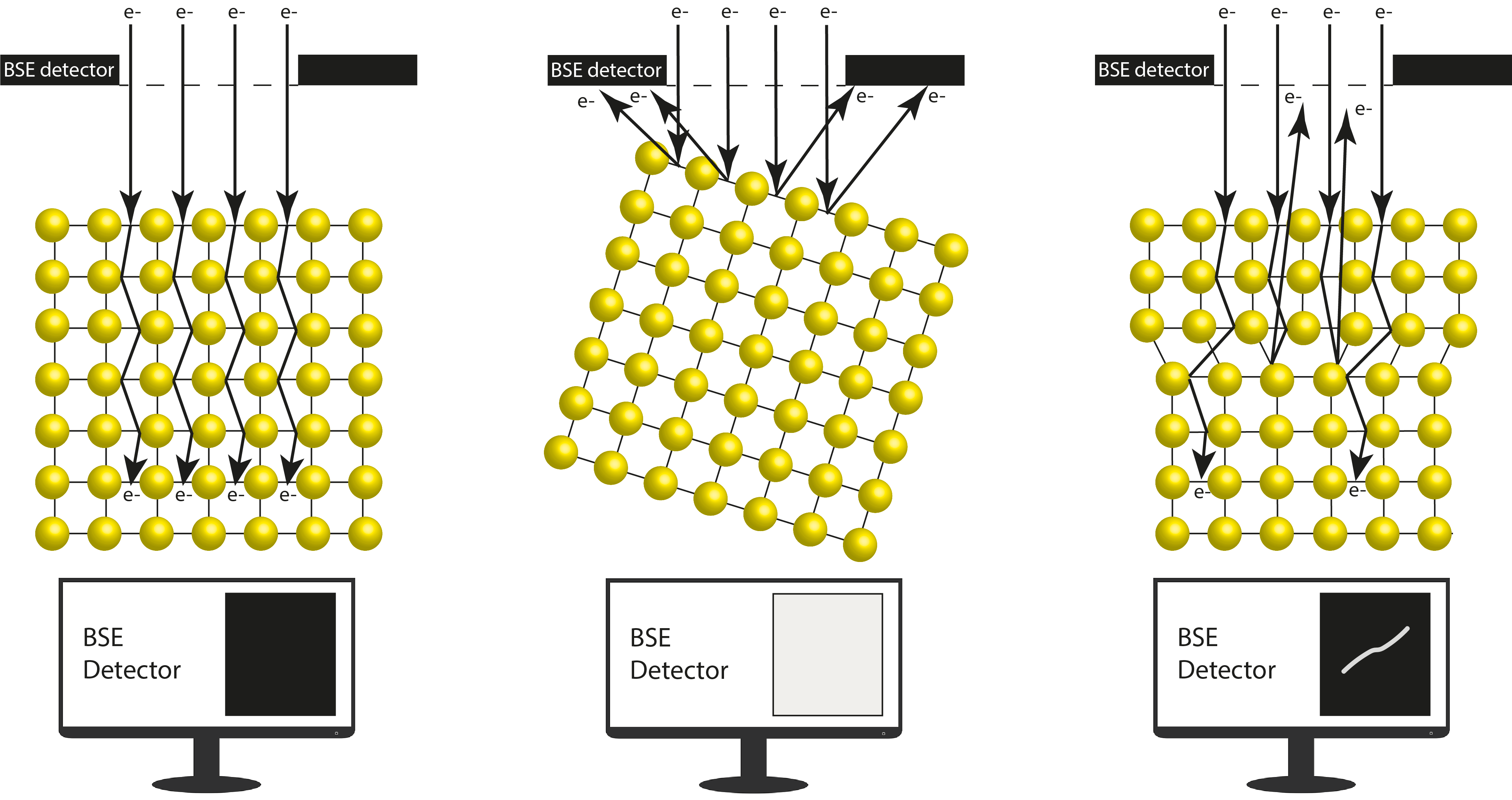
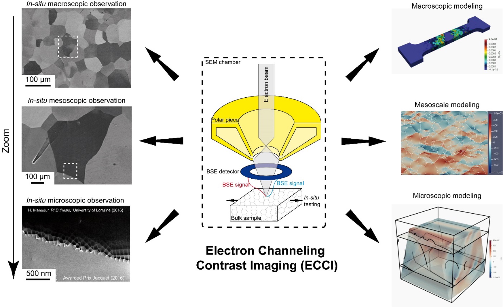
Our SEM specialtyECCI is a non-destructive SEM technique that reveals sub-surface defects in bulk materials with both fine detail and statistical relevance. Unlike TEM — which provides detailed but limited statistical information on defects — ECCI offers comprehensive defect characterization over larger areas in bulk samples without damaging them. It works by detecting variations in electron scattering along crystal planes, highlighting defects up to ~100 nanometres deep. We use ECCI to track how these defects evolve during deformation, and we develop new procedures to further exploit the potential of this technique, aiming for higher resolution and better signal quality.
In Situ Mechanical Testing in the SEM
SEM techniqueWe perform real-time mechanical and thermal tests inside the SEM, including in situ tensile and compression tests at room and high temperatures, as well as nanoindentation. These experiments allow us to observe how materials respond to mechanical and thermal stress, providing insights into their structural, functional, and failure behaviors. By comparing experimental observations with simulations and modeling, we validate and refine predictive models to better understand and optimize material performance.
By combining SEM-based techniques with TEM, we gain a comprehensive understanding of material behavior. I am open to collaborating on new, innovative projects — whether fundamental or industrial — to apply and further develop these techniques.
Selected publications
A selection of publications from this research axis:
Estimation of dislocation densities with non-destructive SEM techniques: application to GaN
Microscopy and Microanalysis, 2025, 31 (1), 1–14 DOIFundamental and experimental aspects of diffraction for characterizing dislocations by electron channeling contrast imaging
Scientific Reports, 2017, 9742 DOI